Tag Archive: serial port


I have a small stack of WRT54G routers at my house.  When I find them second hand for cheap, they tend to be the WRT54G-TM variant.  This version is actually great for modding and hacking because people seem to think it’s tied to T-Mobile so it must require a contract to use or something and they will sell them cheap.  Personally I’ve had no trouble putting DD-WRT on the WRT54G-TM.  In fact, the WRT54G-TM has 32MB ram and 8MB which is far more than most of the other routers in the series.

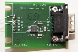
Today, I’m going to add a serial port to my WRT54G-TM so I can use a terminal to log into it.  I think this will be handy for debugging since I plan to change the firmware on this router to Openwrt.  I’m going to use a debugging board given to me by an unnamed friend at an unnamed company.  There is nothing special about the board.  It’s just a serial level shifter with a Maxim 3221CAE IC on it.  It’s a fairly standard circuit that they publish on the datasheet for that IC.  I’m just using this board because it will save me time doing this hack.  The nice thing about the 3221 variant is that it will run on the 3.3V that is already present on the header.  I’m loosely following directions from here showing two serial ports added to a WRT54GS.

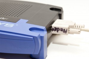
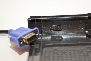
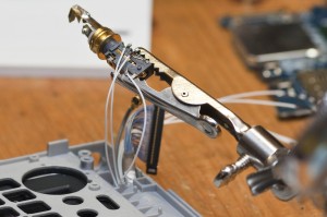
To mark out the location for my new serial port, I’m going to use fire.  I found a totally useless serial dock that corresponds with a defunct proprietary service and grabbed my blowtorch.  I heated up the end of the cable as hot as I could get it and made an impression inside the WRT54G-TM.  After that, I took a Dremel and routed out a hole for the DB9.

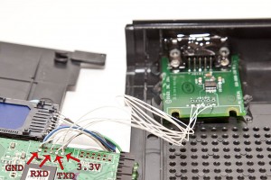
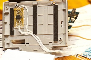
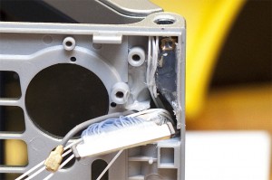
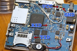
Next I soldered the wires in place.  On the Maxim chip, the r-out goes to the RXD pin on the header and the t-in on the chip goes to the TXD on the header.  3.3V on the header goes to VCC on the chip and GND goes to GND.  Make sure to leave the wires long enough to get the case closed again.  After I was satisfied with the soldering, I globbed on a LOT of hot glue to hold that little serial board in place.  Ignore my sd card mod since it’s not related to this hack.

Once it was all back together I fired up Minicom with the settings 115,200, 8, 1, no parity and no flow control.  The no flow control part is especially important.  Now when I boot up the router, I can see all of the debugging information.  Now with this serial port I can experiment with vlans and other things that can break your SSH session.  If I wanted to get really tricky, I could probably even use my hacked WRT54G-TM as a wireless-serial bridge for consoling into my Cisco routers that I keep in the garage.  They are too loud to keep by my desk.

If you like this article, you can support my site by using this link to buy your next WRT54G from Amazon.  You might also consider buying Linksys WRT54G Ultimate Hacking for more advanced hardware and software hacks for your WRT54G.

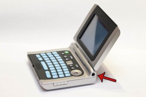
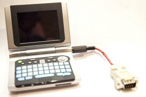
Usually when I modify something, I try not to ruin the aesthetics. It has to perform and look better(or the same) than before I start the project, otherwise I don’t want to do it. I think this mod has achieved that. With some help from a friend, I managed to design and build a surface mount serial level converter board that fits inside the Zipit Z2 behind the screen. It pops out of the Zipit in the form of a 3.5mm headphone jack that is stuffed up in one of the only spots it would possibly fit. From there, I built a short cable that turns the 3.5mm plug into a DB-9 for plugging into any standard serial hardware.

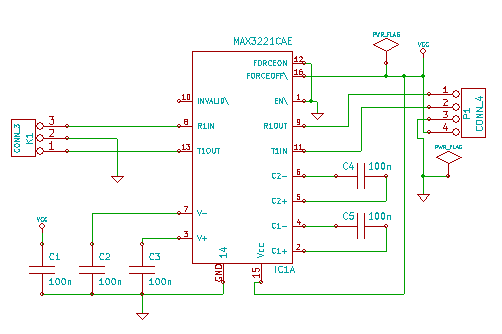
The mod is powered entirely from the Zipit it and will have an unnoticeable effect on battery life. The chip I used is the Maxim 3221 CAE 16 pin SOIC variant which also has some built in power saving functionality. This was the smallest chip that I could find that would do the job. The size of the capacitors on the board are not entirely critical but their function is. They help the IC boost the voltage up to the proper level for communicating with RS-232 devices. Without the caps, chances are that the converter will work for some devices and not for others because it will fail to fall within the RS-232 spec. I used .1uF surface mount caps in a 603 package. They are pretty tiny but certainly not unmanageable. There are plenty of tutorials out there on soldering surface mount components if you happen to be nervous about this.  Here is the schematic.

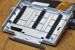
Before we can put the board in, we need to crack the case so I put together this Zipit disassembly guide.  After it was apart, I could see the space that I had behind the screen.  It’s a surprising amount really.  They could have made this thing a little thinner if they wanted to.

Here is a good view of the area behind the LCD

Test fitting the 3.5mm jack

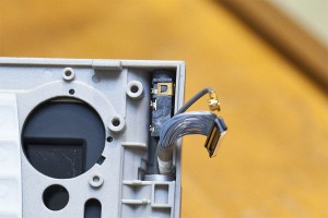
As I was I saying, the 3.5mm jack is stuffed in the only spot I could find for it.  It’s where the LCD cable comes down from the upper half of the Zipit.  I happened to salvage this headphone jack from a Sansa Shaker which is a great MP3 player for a baby.  I had an extra one that was broken so I took the two headphone jacks out of it and gave one to my friend.  rkdavis found a 3.5mm jack on Digikey that looks pretty similar to what I used.  The space is very tight so the size of the jack is critical.

The wires routed and board mounted

As you can see, that board fits perfectly in that empty square.  I used a few dabs of hot glue to hold everything together and route the wires where I wanted them to go.  I took care to mark the wires with Sharpie pen notches so I knew which wire went where.  The wires I used are Kynar 30 AWG wire wrap wire.

Using helping hands to solder the 3.5mm jack

After the wires were all routed, I stuck the LCD housing back together.  I pulled all 7 wires through the same spot where the LCD wiring comes into the lower half of the unit.  I used some Helping Hands to hold the headphone jack and solder tiny wires to it.

3.5mm jack hot glued in place

I used copious amounts of hot glue to make sure that headphone jack didn’t move.  I also drilled the hole extra tight and crammed the jack into it so I don’t expect any movement at all.  After this step, the hard part is done and there are only 4 wires left to hassle with.

Mainboard locations for hooking up the serial converter

I stuck the keyboard back together and put the motherboard back into the zipit it.  Then it was fairly easy to solder the last four leads to these locations and put the bottom half of the case back together.  Now that it’s done, it’s time to plug it into a serial port.

The completed mod including the dongle

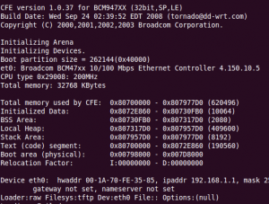
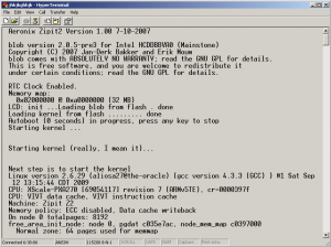
I’m using Hyper Terminal in Windows XP under VM Ware Fusion.  The port settings are 115,200, 8 bits, 1 stop bit, no parity and NO flow control(very important).  Here is what pops up when I first boot the Zipit.

This is what pops up when you first boot the Zipit

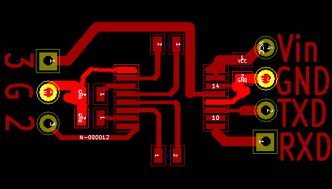
If anyone wants to replicate what I’ve done, here is the PCB layout for Kicad.  Feel free to comment if you need more assistance.

Now for that USB host mod

If you are interested in buying your own Zipit to hack and you like the information on my site, please buy your Zipit using this link and support my site. You won’t find them anywhere cheaper than that anyways.

I’ve been fighting with Kicad to design a tiny little serial converter for my Zipit.  The Zipit needs a serial converter because the outputs inside the Zipit don’t conform to the RS-232 voltage standards and they are unbuffered.  In other words, most RS-232 devices probably wouldn’t recognize them as they sit AND you could inject a voltage spike directly into the CPU if you decided to hot plug a device.  These serial transceivers have some level of resilience built into them that will protect against such spikes.  Some of the information I’m using in this project is coming from this page:

http://zipit2system.sourceforge.net/?page_id=82

I’m going to use a different chip than he does however.  I priced out the chip he spec’d and it was around $8.  Not sure why, there is nothing particularly special about it.  I chose a different chip for my project though.  I’m going with the Maxim MAX3221CAE in a ssop16 package which is ridiculously small and costs less than $2.  There are sixteen pins on the chip and it is roughly 6.3mm long.  This will be perfect because I am going to install my serial board inside the Zipit entirely.  Then I will use a 2.5mm jack to a DB9 cable or something similar to actually hook up to other devices.  The board I’m making will mount inside the lid behind the LCD screen.  Believe it or not, there is plenty of room back there.  My goal will be to make it so that no grinding or cutting is necessary but somewhere along the way I’ll need to drill a hole for the actual port anyways so no big deal either way.  I’d like to keep it looking as stock as possible.

Here is the schematic I designed(with help from James):

A flaw James pointed out with the other serial design is that the charge-pump capacitors were omitted.  This means that the output still may not have properly complied with the RS-232 spec with regard to voltage levels since those are part of the circuit that builds up the voltage.  I’m sure the other design works in most cases but it’s possible there are stubborn, older devices that could choke on it a bit.

Correction 6/25/2010: After looking at the datasheet for the Maxim 3223e, it appears to have internal charge-pump caps.  The chip is still much too large for my purposes but slightly easier to implement because it has fewer external components.

Anyhow, time to etch a board and see if it works.  Wish me luck.

Yesterday I started another little project.  I’m going to add a serial port to my Zipit Z2.  There are lots of good reasons to do this which I will further detail in another blog.  The Zipit Z2 technically has a serial port already on the motherboard but the outputs are not at levels that conform to RS232 standards so I need to add an RS232 transceiver to convert the levels properly.  The chip I’ve chosen is the Maxim MAX3221CAE.  This isn’t a standard dip that I could just throw on a piece of perf board and call it a day.  See, unlike other Zipits I’ve seen serial-modded, I want to fit the whole mod inside of the Zipit.  There just isn’t enough space for a big old dip anywhere in the unit.  My is to use a tiny surface mount 16-pin SSOP on a custom made paper-thin PCB.  Of course this leaves me with needing to design the board.  I’ve hand drawn boards before that use SMT’s but this one is just too tiny to be accurate.

A hand drawn PCB I made a few years back.

For this project, I need to be much more accurate and make a much smaller board to fit the limited space I will have.  This is where I need a software package like Kicad.  Kicad has many different libraries of existing components built into it already and 1000’s more available via packages on the net.  Kicad is NOT straight forward though.  Even if you’ve used something like Autocad or Mastercam in the past, this program has it’s own set of funny conventions that make little sense.  I’m going to give you a short rundown here of the steps I’m using to make my board.  My list will be incomplete and may not work for you but it’s meant to just be a general outline of the steps you need to go through to get a board made.  My friend James was kind enough to sit down with me for a couple hours and walk me through this program so my list here is made from memory and from notes I made during that short training from him.

  1. Open up Kicad and create a new project.  Give it a name and ignore the warnings.
  2. Now that you have the main window open, add your devices to the board.  The device tool near the top of the right-hand toolbar.  After you’ve selected the device tool, click somewhere with the cross-cursor.  Chose “by lib browser”, find your component and then hit the “x” to close that dialog.  The cursor turns into the component.  Now click somewhere to place it.
  3. After you’ve placed it, you can change the placement and orientation by putting your mouse over it and pushing “r” to rotate or “m” to move it.
  4. After you’ve placed your components, push the “add wire” button below the device button.  Draw in all your wires and make sure you don’t have any goofy junctions.  Save your drawing!
  5. Now hit “Netlist generation”.  It’s in the top menu near the right-hand side.  Hit netlist, generate it and save it.
  6. Right click on every component you placed and annotate it.  Stuff like IC1, IC2, C1-C10, R1, etc.  Giving the parts values is not a bad idea either.  It may help later or if someone else needs to modify or view your drawing.  There is an auto-annotate function but it’s not my preference.  Save again.
  7. In the top menu, push the “Run CVpcb” button.  It’s orange and near the middle.  In this dialog, you need to associate every component with a package type.  This can be challenging if the type of package you need doesn’t exist as a default.  Save that before exiting.
  8. Run PCBnew, ignore the warning.  Check the measurement units on the left side.  Pick inches or mm.  Turn on the rat’s nest below the measurement tool if it isn’t on already.  Click “read netlist” on the top of the screen near the middle.  Click “read current”.  Now your parts are stacked in a blob in the corner.  Draw a box around them with the pointer and move them towards the middle of the sheet.  Click “ok” on the dialog.
  9. Zoom in and mouse over the blob of components.  Hit “m” and move components off the stack one by one.  As you move them, hit the “r” button to rotate them into place.
  10. Route your tracks.  Right click to end.
  11. Select the PCB edges layer and draw your PCB.  This can also be the first thing you do.
  12. You should now have a printable board.  I’ll report back when I do but it could be a while.

I realize this list may have small discrepancies or may be flat out wrong.  There are several tutorials online that explain it better than I do but mine is just to give you a really quick overview of what it will take to actually draw a board with this tool.  Please email me or comment if you see any glaring errors.  I will be on my way now to rip my hair out after using this incredibly complex and confusing piece of software.

Powered by WordPress. Theme: Motion by 85ideas.